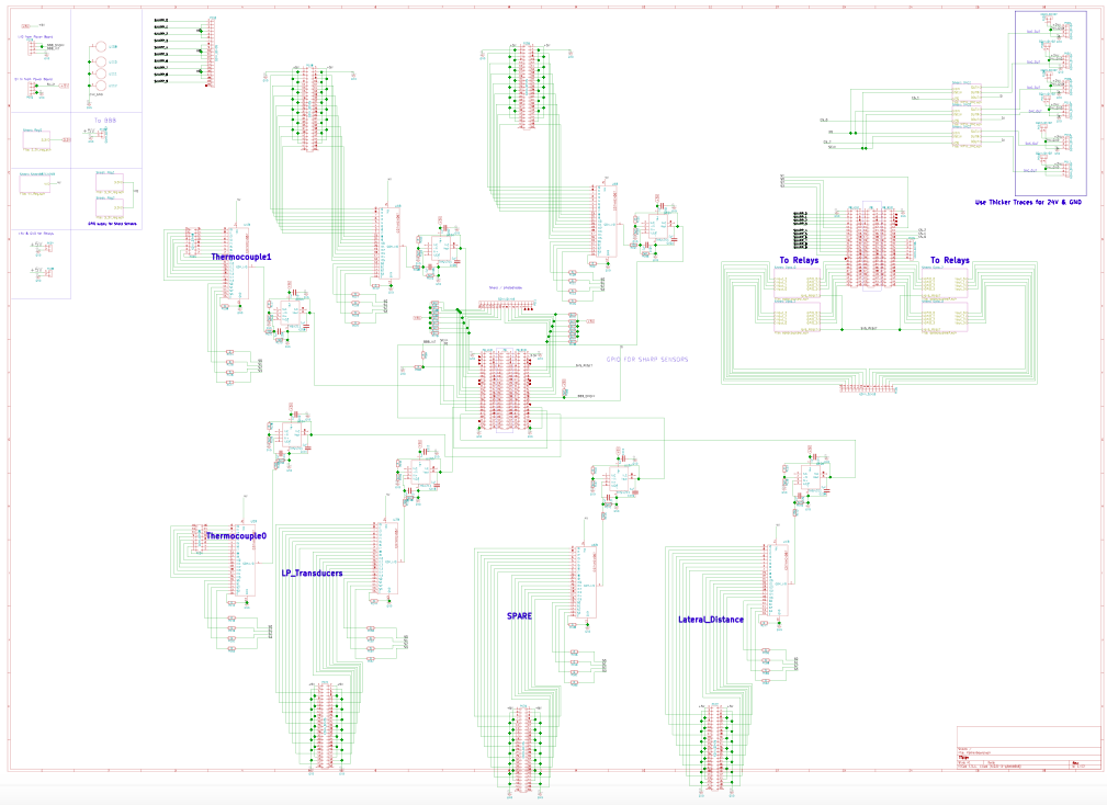
The Motherboard
Can you tell that was my first schematic? It hurts to look at now.
All of these files are on Github with tags for each version we deemed final enough to procure. We did our best to be good git stewards but still managed to break the repo once or twice.
Rev 1.2
I have so many questions for my past self
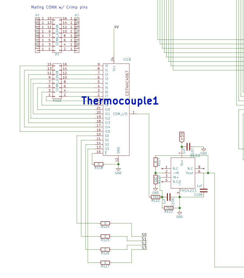
The main function of this board is to collect all of the analog signals around the Pod. The circuit in is reused multiple times. An analog MUX is used to select an analog channel, which is fed through a buffer to the flight computer's (Beaglebone Black) internal ADC for conversion. There were numerous areas to improve this solution.
- The circuit doesn't take into account the 90-200 Ohms of resistance from the MUX
- The buffer has a mix of sensor types coming in, each with different frequency characteristics
- Definitely didn't simulate the op-amp.
- The Beaglebone Black has a max ADC voltage of 1.8V. Most of the sensors are 0-5V scale
- At a systems level: we never considered crosstalk and other errors on the line due to switching.
- I picked an $8 op-amp for no other reason than "high speed". At least I buffered the ADC?
- The MUX can accept 5V.. I'm not sure why I went to the trouble of making another rail
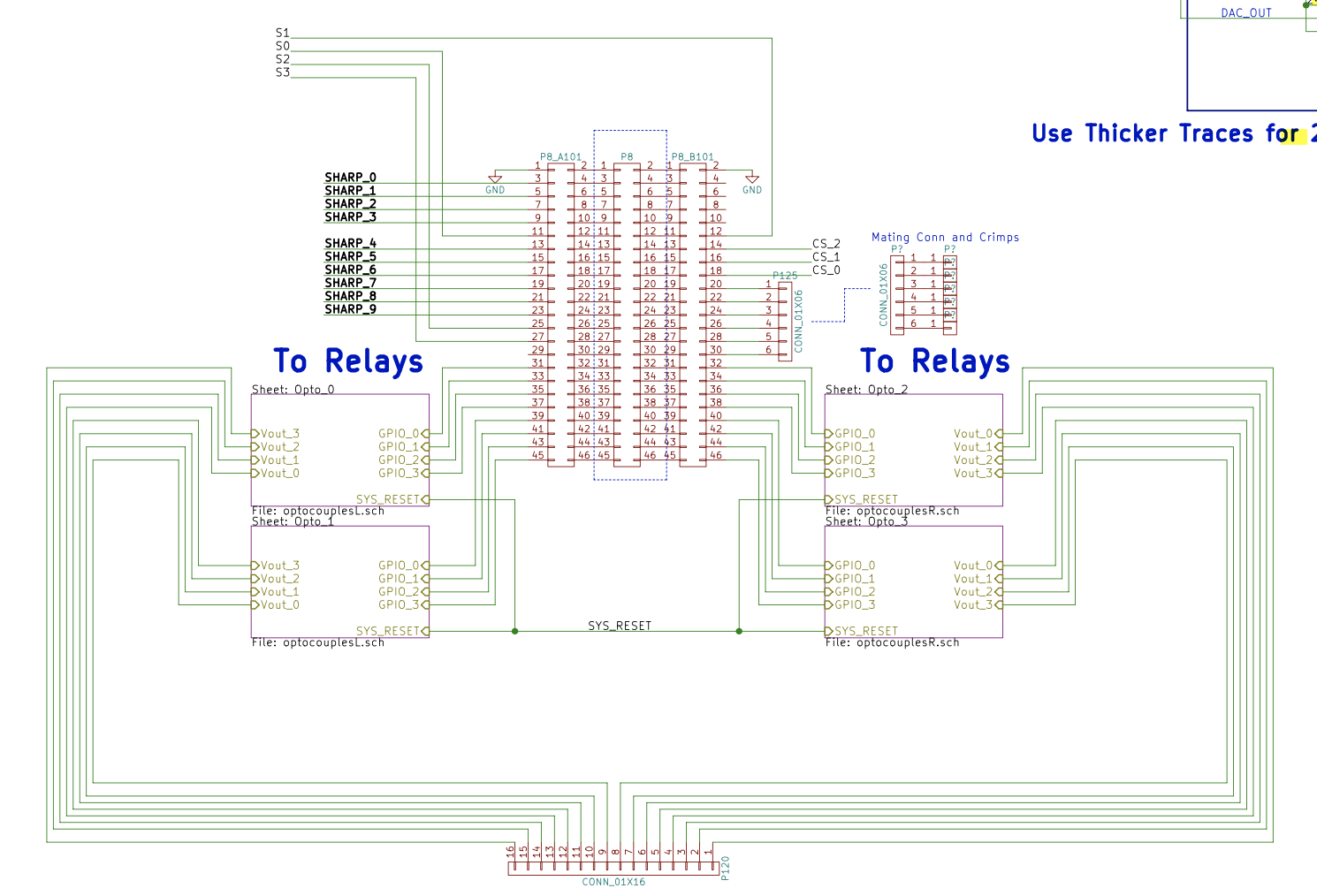
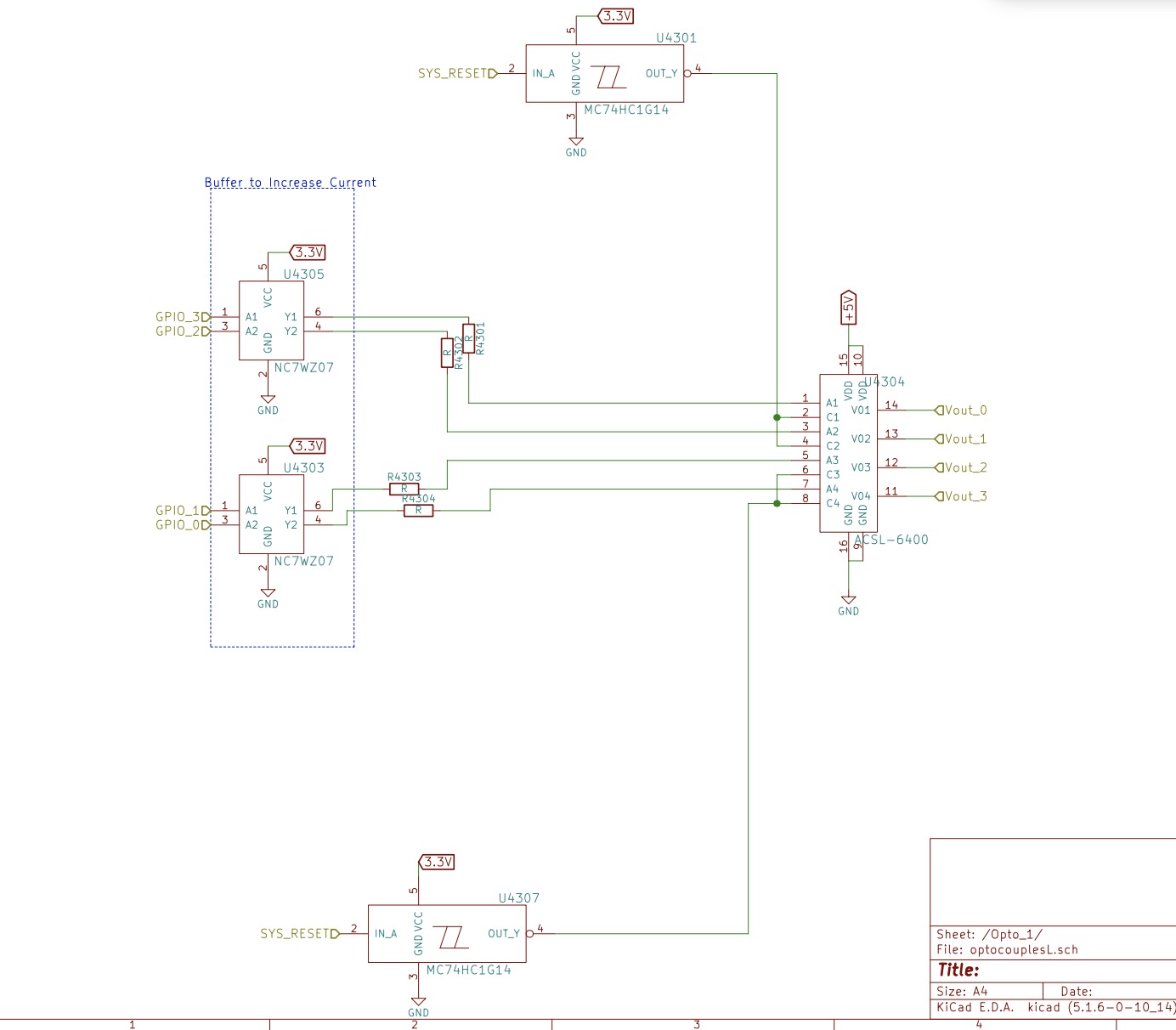
The first iteration of this board just about maxed out the GPIOs on the Beaglebone. (this is from memory.. need to
double check) These pins have some special functionality when used for display applications and have quirks on boot. They boot
in an indeterminite state and we were concerned the relays could intermittently be fired. So we decided to use... a Schmitt Trigger
inverter that is triggered by the Beaglebones POWER_GOOD signal to sink each optocoupler cathode. The GPIOs are fed through a noninverting open drain buffer.
This shouldn't work. There are no pullups and return current is going into the inverter?
- The 3V3 rail has two regulators on the same net to boost available current. I should have picked a better part.
- The DACs were 3x3mm QFNs that we had zero business trying to solder on to the board
- All of the power is a label or global net instead of a proper power flag. One mispelling and a rail would be toast.
- General use of hierarchical sheets is just wrong.
We compiled all of our lessons learned after Competition I and went back to work. The motherboard was brought up to Rev 2: The Motherboard Rev 2.