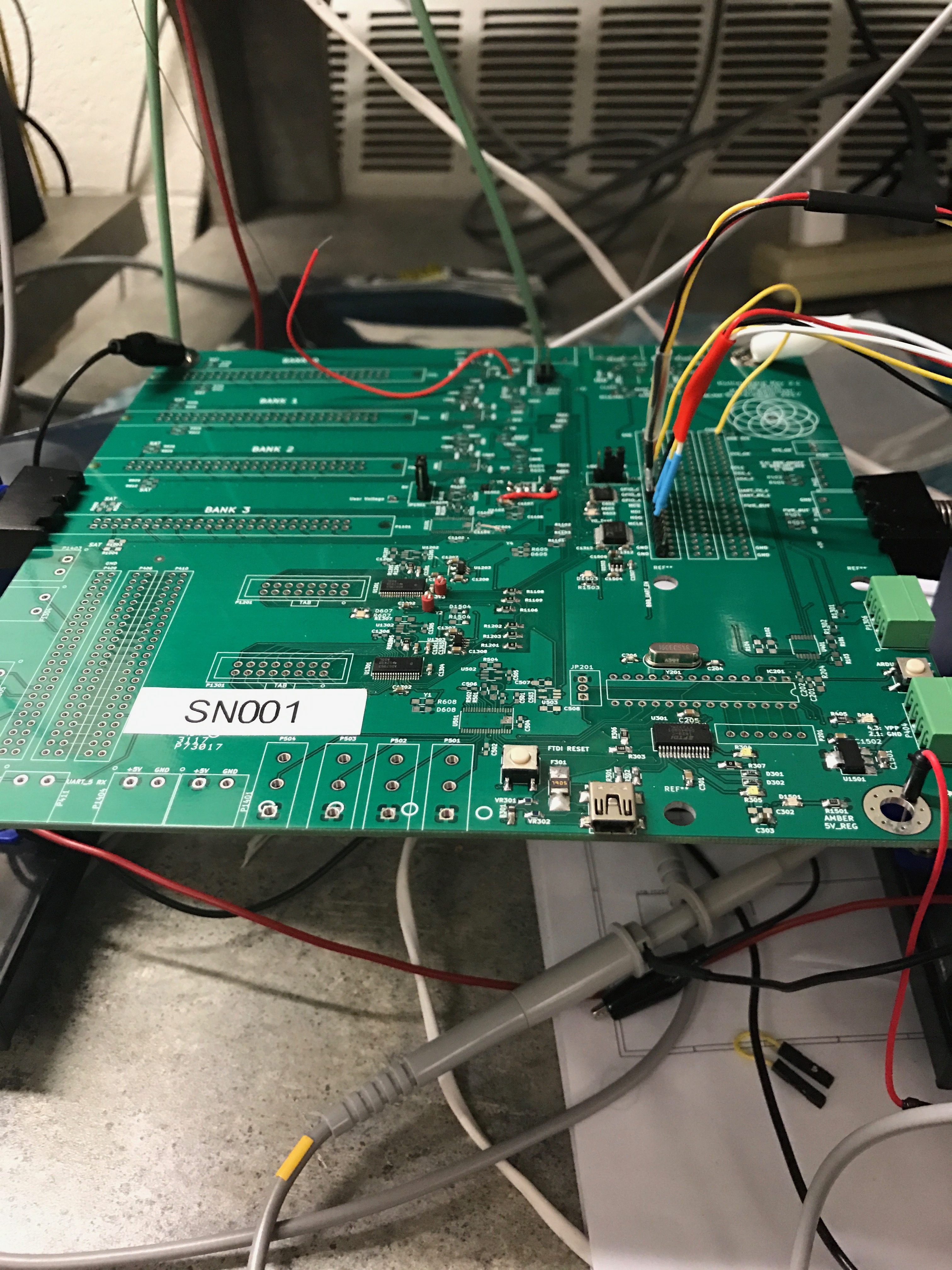
Rev 2.1
Months of research and co-op helped improve this schematic quite a bit! It is certainly not perfect, but pretty good for a revision.
All of these files are on Github with tags for each version we deemed final enough to procure. We did our best to be good git stewards but still managed to break the repo once or twice.
Analog -> digital
Some problems from R1.x were hammered out
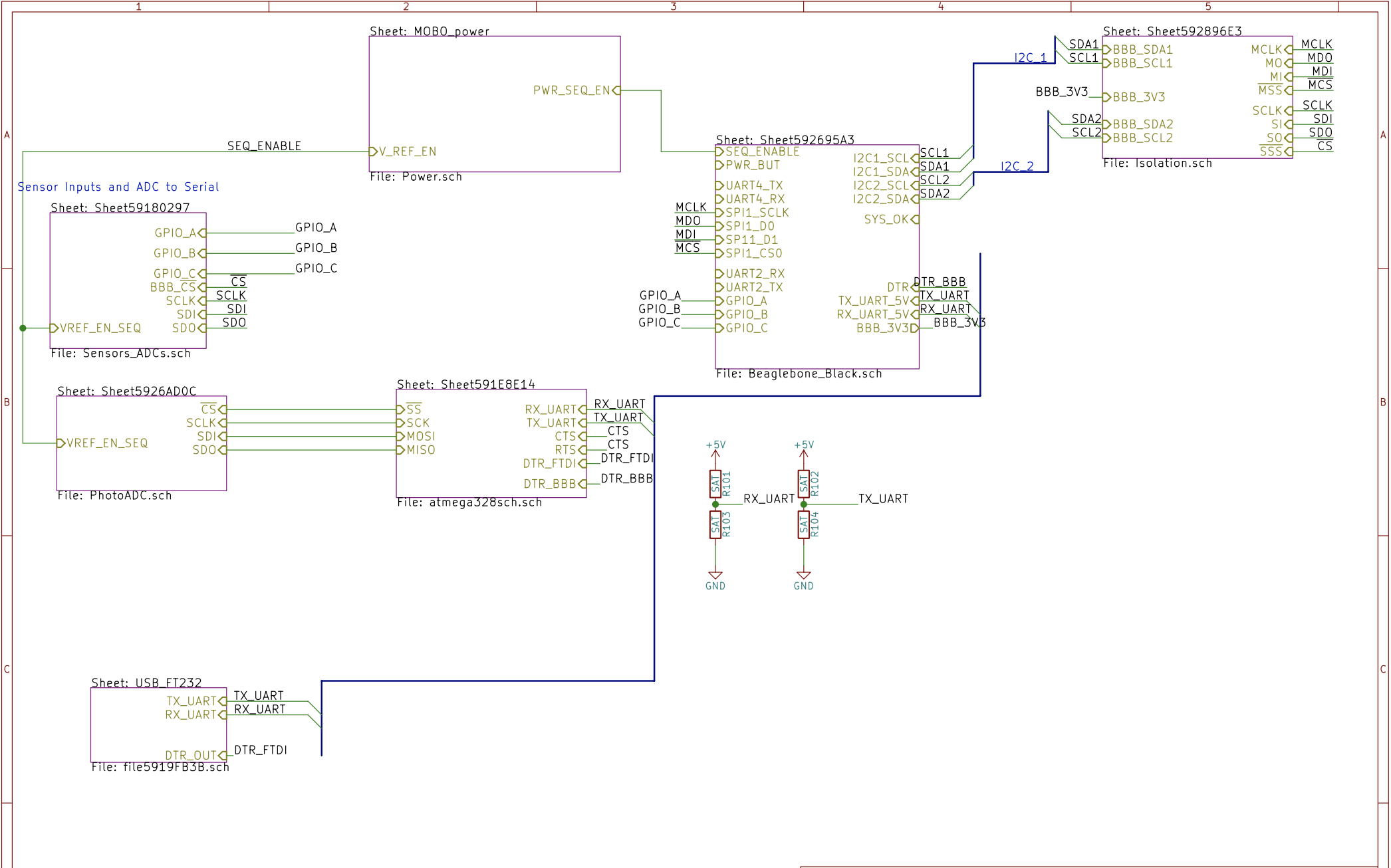
All of the lessons learned from a board and system level were pulled into the redesign of the entire system, but the Motherboard had significant changes.
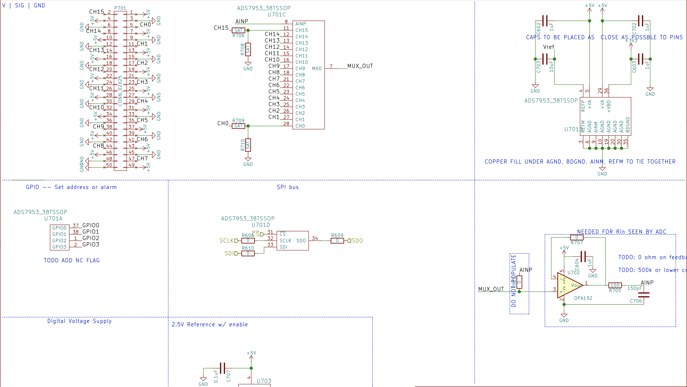
- The analog MUXs were swapped for fancy ADCs.
- Power sequencing/enables to properly turn on the ADCs
- Each ADC bank had similiar sensors, so a corner frequency could be designed into the buffer.
- There's resistor divider slots in case one or two signals need to be dropped.. not perfect but adds flexibility
- We did extensive testing, across the electrical team, with breakout boards before pulling into larger designs.
- The MUX resistance is still an issue. It was considered but left in favor of more analog channels
- The features of this ADC save pins and processing on the BeagleBone.
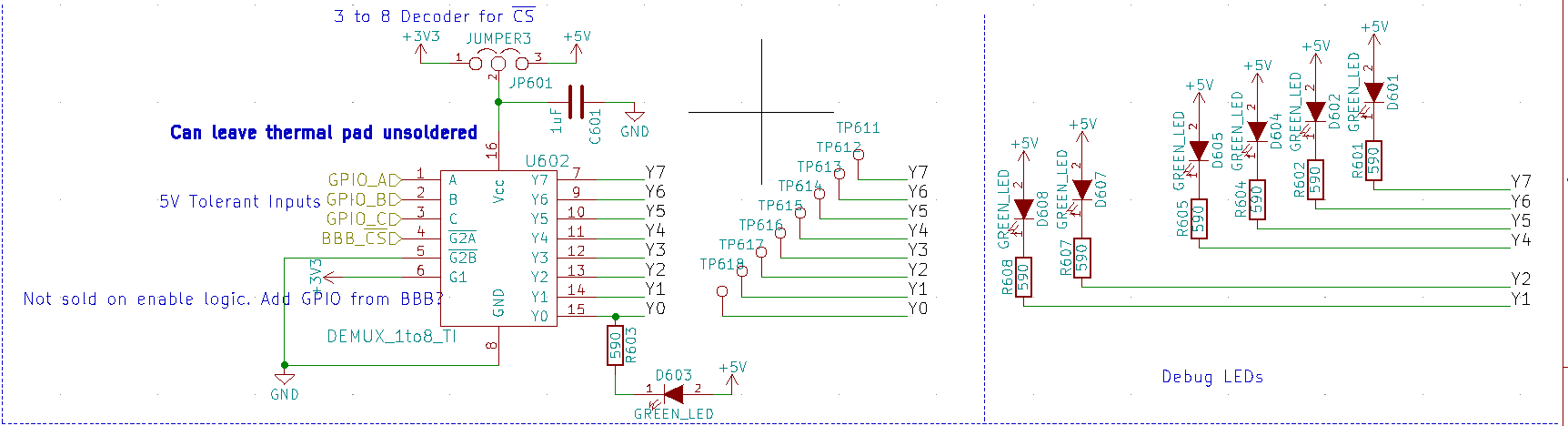
There are so many ADCs on the SPI bus that a decoder is used to save Beaglebone pins for the chip selects. The LEDs
are used for bring-up and software development, not for "flight" units. Initially the clock is as slow as possible
to ensure all of the addresses map correctly. These LEDs were probably pretty detrimental to operation and it
probably should not have worked. I guess the ADC CS pin is sinking the extra current?
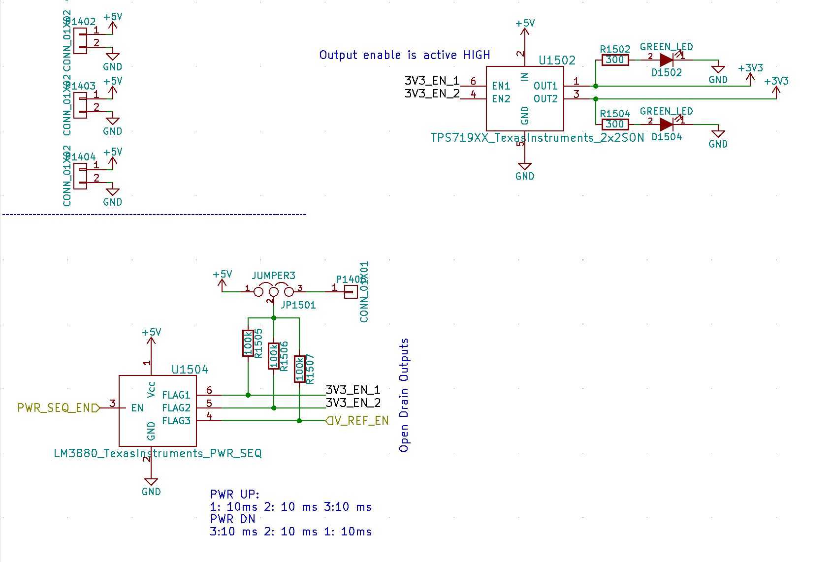
One pain point for the ADC is some interesting behavior during testing. It locks up when supplies are not brough up in the right order. AVCC must always be greater than DVCC, but the VREF also has a play in the timing. The latter isn't in the datasheet but it is fixed by turning on analog-> digital -> VREF. A power sequencing chip ensures the Beaglebone has time to boot, then the beaglebone enables the rails. the issue. The 3V3 rails are not tied together this time. Each output powers half of the ADC bank, but they should have been designated A or B.